OptaCap Technology Click here to download
white paper
The Benefits of PlasmaSi�s
Revolutionary OptaCap� Technology
In
contrast to conventional PECVD technologies, PlasmaSi�s OptaCap� offers
superior, scalable Thin Film (TF) barrier layers produced at high growth rates at
very low temperatures, with single chamber, multi-layer capability and the
lowest cost to date among deposition technologies.
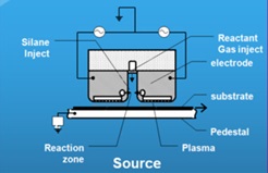
How PlasmaSi Source works:
1. Reactant gas containing
nitrogen is injected from the top of the gap into the plasma between electrodes
towards the substrate.
2. As it flows down in the plasma
it breaks down into Nitrogen atoms and activated N2 molecules.
3. The Silane is injected near the
bottom of the electrodes and reacts very quickly with the high concentration of
active nitrogen species to form SiH2(NH), Si3N4 and other SiN compounds.
4. The
reactions going to completion as the mixed gas reaches the substrate result in
deposition of substantially Si3N4 material on the substrate and very little NH
or SiH compounds incorporated into the barrier film.
Strengths of PlasmaSi�s OptaCap� technology
include:
� Sub-80� silicon nitride deposition.
� Meets OLED industrial requirements as a moisture barrier.
� High productivity through high deposition rates.
� Excellent uniformity of rate and material properties across large substrates.
� Low defects due to a deposition head design that eliminates gas phase particle formation.
OptaCap� Product Click here to download product
specification
PlasmaSi will deliver three different solutions to the market place :
� The first type of system is for Gen 2 panel-by-panel in-line deposition for encapsulation of display and lighting products on rigid substrates.
� The second type of system performs plastic roll-to-roll web coating depositing PlasmaSi�s thin films on plastics webs for various applications.
� The third offering is PlasmaSi�s Core Deposition System that consists of at least two plasma sources per head along with associated RF power and gas supply systems.
The Core Deposition Head, which is a cluster of plasma sources in parallel along with the associated RF power and gas supply systems, has been optimized through extensive experimentation and modeling procedures. Because the source technology is linear, it is much simpler to scale to substrates of larger sizes compared to conventional parallel plate systems thereby enabling performance superior to that of competing deposition technologies.
� The Deposition Source�s linear geometry allows PlasmaSi to design components so gas properties and RF power have less variation along the source length. This design has led to more uniform deposition rate and film properties and is easily scalable to very large substrate sizes.
� The Deposition Source does not grow tensile films on its walls enabling in-situ plasma cleans. In-situ cleans are highly effective in extending intervals between preventive maintenance in mass production.
� The reactor can easily be made modular with a dozen or more Core Deposition Heads per chamber.
Below, a schematic cross section is shown of a single source as configured in our R&D system. The source can, as required, perform deposition of the same or different materials within this chamber. This means that the cost of the depositing film stacks can be substantially reduced. The above benefits of PlasmaSi�s OptaCap� technology have been demonstrated with multiple display manufacturers.
For
more information, please contact with us [email protected]
[top]