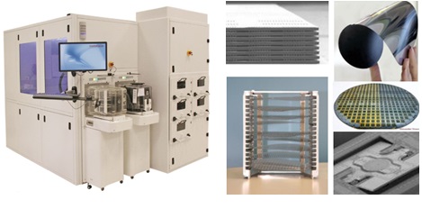
Features:
- Wafer size: 8"/12� (or 6�/8)
- handling of standard, thin, warped, eWLB, Taiko and MEMS wafers
- highest level of reliability and availability
- two 6 axle robots for optimized footprint
- up to 8 stations for shipping boxes and packing material
- automatic end-effector changing station
- two load-ports
- mapping sensor
- pre-aligner for 8"/12" (or 6�/8�)
- SECS/GEM interface
- CE certificated
- SEMI standard compliant
Applications:
Wafer Loader:
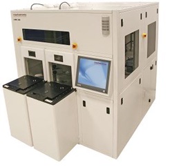
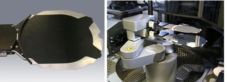
II. Wafer Loader mWL 200/300
(150/200)

The Wafer Loader mWL 200/300 is designed for fully automated loading and unloading of 8"/12" (or 6�/8�) wafers or frame cassettes from FOUPs/FOSBs onto an external chuck.
The adaptation to OEM tools according to customer requirements is possible.
Features:
- Wafer size: 8"/12" (or 6�/8�)
- handling of standard, thin, warped, eWLB Taiko and MEMS wafers
- handling of frames
- highest level of reliability and availability
- optimized footprint
- automatic end-effector changing station
- two load-ports
- mapping sensor
- pre-aligner for 8"/12" (or 6�/8�)
- SECS/GEM interface
- CE certificated
- SEMI standards compliant
Applications:
- loading/unloading on a chuck
- wafer handling automation (e.g. for process, inspection, metrology tools etc.)
TAIKO Ring Remover:
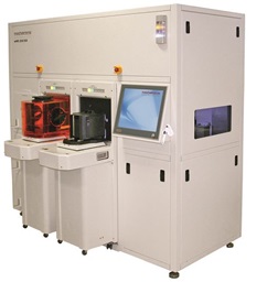
III. Ring Remover mRR 300 (200)
The Ring Remover mRR enables fully automated handling of film frames and removing pre-cut rings from the laminated wafer 12" (or 8�).
Features:
- Wafer size: 12" (or 8�)
- throughput up to 60 wafers on film per hour
- highest level of reliability and abailability
- optimized footprint
- two ring remover stations
- two load-ports
- SECS/GEM interface
- CE certificated
- SEMI standard compliant
Applications:
Wafer Sorter:
IV. Wafer Sorter mWS 200/300
(150/200)
The Wafer Sorter mWS 200/300 is designed for sorting 8�/12" (or 6�/8�) wafers and can be equipped with up to four cassettes or FOUPs (mixed loading possible).
The mWS 200/300 handles wafers out of a cassette / FOUP onto a pre-aligner, forward onto a visual inspection unit and back into a cassette / FOUP.
Features:
- Wafer sizes: 8�/12� (or 6�/8�)
- handling of standard, thin, warped, eWLB, Taiko and MEMS wafers
- highest level of reliability and availability
- one dual arm robot on linear track
- up to four load ports
- wafer flipping function
- automatic end-effector changing station
- mapping sensor
- pre-aligner for 8"/12" (or 6�/8�)
- SECS/GEM interface
- CE certificated
- SEMI standards compliant
Applications:
Components?
End-Effectors:
I. Bernoulli Vacuum
End-Effectors
The Bernoulli vacuum end-effectors (mBV series) are designed for back side handling of thin and warped wafers, e.g. for handling from the cassette to the pre-aligner.
Types according to wafer
size:
Function:
The Bernoulli vacuum end-effectors use Bernoulli air-flow and vacuum one after the other. For flattening the warped wafer in the cassette a short burst of clean dry air (CDA) or nitrogen is applied to bring the wafer into the right position. Via vacuum the wafer is secured on the end-effecto.
Features:
- Wafer sizes: 6�, 8�
- For thin-wafers > 50 �m (2 mil)
- Warped wafer handling (up to 12 mm warpage)
- Back side handling
- Bernoulli airflow and vacuum
- Automated quick coupling
- Automated loading and unloading of several
mechatronic components
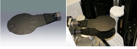
II. Contactless End-Effectors
The contactless end-effectors (mCL
series) are designed for contactless chip side & back side handling of thin
and warped wafers, e.g. out of and into a cassette.
Types
according to wafer size:
6� (mCL 150)
8� (mCL 200)
12� (mCL 300)
Function:
The contactless end-effectors use only Bernoulli airflow (no vacuum). The wafer is hovering on the air cushion 0.2 - 0.3 mm above or below the end-effector and is limited sideways by PEEK-elements.
This end-effector does not require the wafer to be fully planarized. Even warped wafers which are too stiff for other systems can be handled.
Features:
- Wafer sizes: 6�, 8�,12�
- For thin-wafers > 50 �m (2 mil)
- Warped wafer handling (up to 12 mm warpage)
- Chip side and back side handling
- Contacless handling with Bernoulli airflow
- Wafer detection with capacitive sensing
- Automated quick coupling
- Automated loading and unloading of several mechatronic components
- Antistatic surface
Chucks:
III. Thin wafer chuck
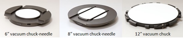
mechatronic vacuum chucks (mVC) are designed for secure placement of various wafer types (eg. standard, (ultra-)thin/warped, eWLB, Taiko, film-frame, MEMS) in a defined orientation. These chucks are mainly integrated in OEM-equipment (eg. for inspection measurement, defect detection �) under atmospheric conditions.
By using a special porous ceramic, the wafer is held on its backside without contacting the wafer chipside. The vacuum holding force is evenly spread on the entire backside surface to flatten the wafer.